


Professional’s Ranking
Professionals
- Limitless simultaneous connections
- Independently licensed no-log coverage
- First rate world server unfold
Cons
- Month-to-month membership is expensive
- Not all servers work with streaming providers
Our Verdict
IPVanish gives glorious server unfold and limitless simultaneous system connections. The options it brings to the desk are sturdy, however its interface tends to lag a bit. General its a stable VPN with nice pace and its no-log coverage, just lately confirmed by way of third-party audit, has made the service much more enticing for the privateness aware.
Greatest Costs In the present day: IPVanish VPN
IPVanish in short:
- P2P allowed: Sure
- Limitless system connections: Sure
- Enterprise location: United States
- Variety of servers: 2,000+
- Variety of nation places: 75+
- Price: $11.99 monthly or $47.89 for a yearly subscription
Only a few VPN providers truly personal their very own server networks and that’s the place IPVanish stands out. As a substitute of counting on business server farms, U.S.-based IPVanish prides itself on operating its personal {hardware} and servers. They even declare that operating their very own server infrastructure makes them a “top-tier VPN service.” In our check, we took IPVanish for a spin to see if it will probably actually reside as much as that self-proclaimed title.
Notice: This assessment is a part of our ongoing roundup of the very best VPN providers. Go there to be taught extra about competing merchandise, what to search for in a VPN, and shopping for suggestions.
IPVanish: Options and providers
IPVanish most important connection display screen with world map and information up and information down graph.
Sam Singleton
At first blush, IPVanish has a clear, if somewhat muted interface. The preliminary display screen you’re offered with is a fast join dashboard with a world map that lets you select your server location and bounce proper in. On the backside of the dashboard you may see fundamental details about your connection together with the server location, IP deal with, connection standing, protocol used, and information up and down. Whereas it could not have any fancy design aptitude, the interface is intuitive and intensely person pleasant. I did word nevertheless that the appliance itself appeared to lag or take an uncommon period of time to load issues, akin to if you transfer or zoom in on the map. First time connections to servers I had by no means used earlier than additionally appeared to take longer than ordinary to attach.
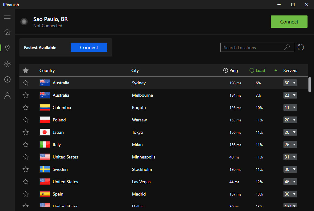
IPVanish location tab with detailed server data.
Sam Singleton
There’s a toolbar on the left of the appliance’s interface with choices for Places, Settings, Information, and Account. Underneath the Places tab, you’re capable of entry extra detailed details about every server together with every location’s ping, load (quantity of server utilization from present person connections), and variety of servers accessible in that location. Additionally they have a useful filtering mechanism that lets you discover the servers with the least ping or load. There are over 2,000 servers everywhere in the world to select from on IPVanish, which is a big step up from just some years in the past once they had lower than half of that.
The truth is, IPVanish has made nice strides lately to replace and optimize its providers. It now helps most main working techniques together with Home windows, macOS, iOS, Android, Chrome, Linux, and some others. That is on par with a lot of the different high VPN suppliers.
IPVanish at present doesn’t have a browser extension, nevertheless it does provide entry to an in-browser SOCKS5 Proxy, which isn’t encrypted like a VPN connection, however does can help you nonetheless reroute your browser’s site visitors by distant servers.
IPVanish has additionally improved just lately in its location-spoofing talents. In earlier years, we seen that IPVanish servers had been regularly blocked when attempting to entry location-restricted content material in different nations. The corporate has evidently stepped up its recreation and throughout the assessment interval there have been only a few noticeable blockages whereas attempting to entry Netflix from quite a lot of IPVanish servers all through the world. Take this with a grain of salt, nevertheless, as Netflix and different streaming providers are continuously attempting to dam identified VPN IP addresses, making it a cat-and-mouse recreation that might change one other person’s personal private expertise.
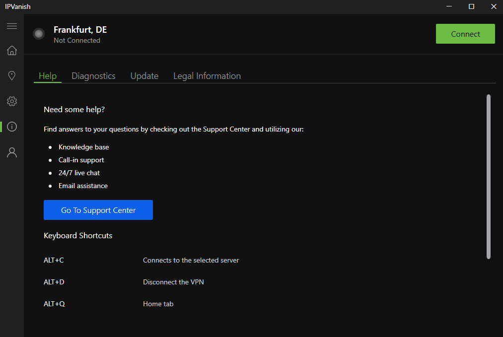
IPVanish 24/7 Buyer assist in Home windows app.
Sam Singleton
The corporate additionally does an excellent job with its buyer assist. It has a built-in assist contact hyperlink instantly from the app. Moreover, it provides 24/7 reside chat assist and a name middle that’s open on daily basis of the week. Its app even helps a number of languages akin to English, Spanish, French, German, and Dutch. These are all welcomed additions lately that present the corporate is attempting onerous to enhance the total scope of its providers.
IPVanish: Efficiency
IPVanish
With claims of getting a superior community, how does IPVanish maintain up in pace exams? Rather well, truly. Evaluating speeds throughout 5 totally different nations’ VPN server connections, IPVanish scored a formidable common of 59 % of the bottom obtain pace and 54 % of the bottom add pace. That places it firmly within the high 5 speediest VPNs we’ve examined.
These comparatively excessive speeds ought to be lots quick sufficient to stream all the high-resolution video or video games throughout most nation connections. Please word nevertheless that this can be a single expertise on a restricted variety of machines, and your expertise could differ.
IPVanish: Safety and privateness
Being primarily based within the U.S. like IPVanish might probably result in privateness issues. This is because of sure home legal guidelines requiring that VPN corporations log and retailer consumer info within the occasion that they’re wanted by legislation enforcement. However IPVanish guarantees to maintain your information completely safe by not logging or sharing consumer info in any respect.
This has been validated just lately when IPVanish allowed a third-party audit of its providers which was carried out by Leviathan Safety group. The audit confirmed the claims that IPVanish doesn’t hold logs of consumer information by any means. It’s not on a regular basis {that a} VPN supplier is keen to place themselves by that type of scrutiny to substantiate its claims.
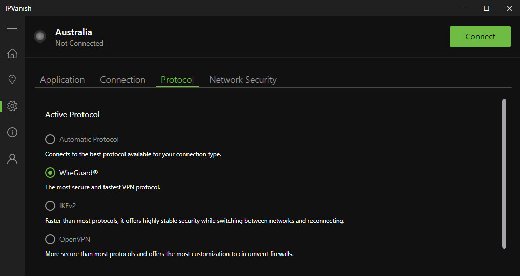
IPVanish has quite a few Lively Protocols to select from so you may customise your connections.
Sam Singleton
IPVanish additionally helps quite a few protocols akin to WireGuard, IKEv2, and OpenVPN. It provides the extra choice to customise OpenVPN connections, permitting you to additional tweak and optimize your connection setup.
Whereas utilizing its service, all the things is encrypted with AES 256-bit encryption which, whereas glorious, is the usual for many VPN suppliers these days. The Home windows consumer comes with IPv6 and DNS leak safety—which our exams verified to be true utilizing each DNS leak check and IPleak.web throughout all connections. Which means that your true location isn’t being by chance leaked whereas linked to its servers.
The IPVanish VPN service comes with just a few additional perks as nicely. It gives an computerized kill swap which is able to disconnect you from the web within the occasion that your VPN connection is severed. Additionally, the VPN comes with an antivirus program referred to as VIPRE. It’s your normal run-of-the-mill antivirus nevertheless it’ll nonetheless block malware and different threats in your pc—sadly it isn’t accessible for cellular variations.
IPVanish: Remaining ideas
IPVanish is a really interesting VPN primarily based in the US. Its connection speeds have jumped by leaps and bounds since our final assessment and it’s now firmly entrenched amongst our quickest VPNs. The desktop app has additionally been improved with an interface redesign that’s simpler to navigate. A latest third-party safety audit is a refreshing signal that IPVanish is assured in its providers and keen to show it to customers. At just a bit beneath $50 for a yearly subscription the value can be onerous to beat. Many individuals may gravitate to extra outstanding VPN suppliers, however IPVanish shouldn’t be ignored. Its latest enhancements present a willingness so as to add options that customers need whereas regularly bettering yr by yr.
Editor’s word: As a result of on-line providers are sometimes iterative, gaining new options and efficiency enhancements over time, this assessment is topic to alter so as to precisely replicate the present state of the service. Any adjustments to textual content or our ultimate assessment verdict shall be famous on the high of this text.