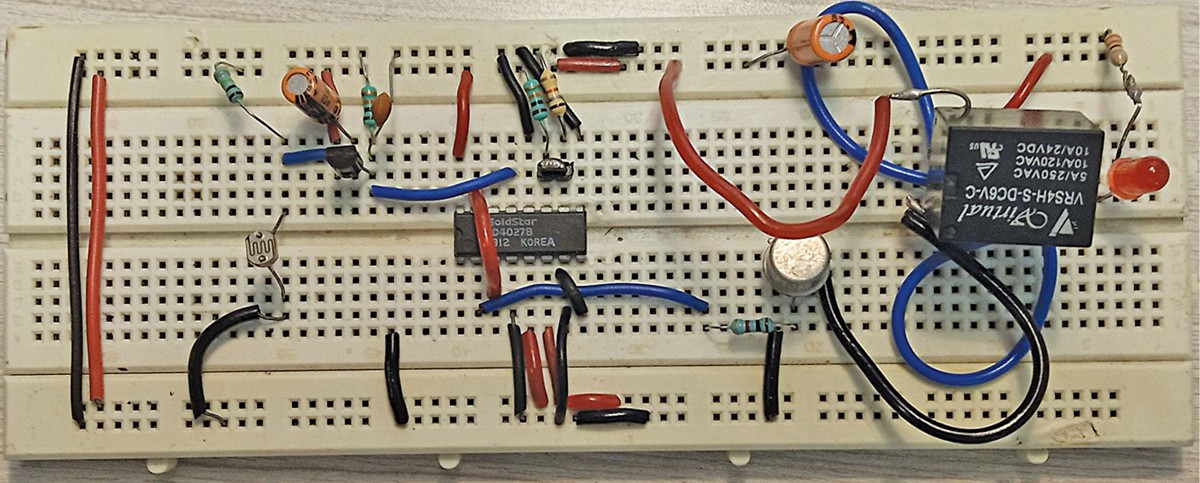
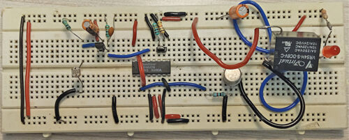
 Specifically Abled individuals, with out arms or ft, typically discover it tough to modify on an equipment. This swap can come to their rescue. It may be operated with a torch gentle or a laser gentle by those that are unable to make use of their ft, and with a footswitch by those that are unable to make use of their arms, to function residence home equipment, fixtures, toys, studying units, and different devices. The writer’s circuit wired on a breadboard is proven in Fig. 1.


Circuit diagram of the swap for the specifically abled is proven in Fig. 2. The circuit contains a bridge rectifier (BR1), 12V voltage regulator 7812 (IC1), twin flip-flop 4027 IC (IC2), 12V one-changeover relay (RL1), a foot swap (S1), and some different parts. Capacitors related throughout the provision terminals are used to minimse any noise indicators.
A mains 230V AC main to 15V, 500mA secondary transformer (not proven in Fig. 2) could also be used to step down the AC mains voltage to 15V AC. This voltage, related throughout CON1 within the circuit, is rectified by bridge rectifier BR1 and filtered by capacitors C1 and C2 to take away any ripples within the voltage. The rectified and filtered voltage is then regulated by IC 7812 (IC1) to offer 12V DC to function the circuit.
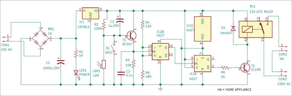
The LDR’s resistance varies with the depth of sunshine falling on it. When the sunshine falling on LDR will increase, the LDR resistance decreases, and when the sunshine falling on LDR decreases, its resistance will increase. In darkness, when there is no such thing as a gentle, the resistance of LDR is within the vary of mega ohms, however in presence of vivid gentle it decreases to some hundred ohms.
IC 4027 has flip-flops IC2A and IC2B which might be used for information storage. IC2C is its energy provide terminal. The sq. wave generated by flip-flop IC2B is coupled to flip-flop IC2A, whose output is given to relay driver transistor T1 to drive relay RL1.
| Components Record | |
| Semiconductors: | |
| IC1 | – LM7812, 12V voltage regulator |
| IC2 | – 4027 twin flip-flop IC |
| BR1 | – 1A bridge rectifier |
| T1 | – BC557 pnp transistor |
| T2 | – SL100 npn transistor |
| D1 | – 1N4007 rectifier diode |
| LED1 | – 5mm LED |
| Resistors (all 1/4-watt, ±5% carbon): | |
| R1, R6 | – 1-kilo-ohm |
| R2 | – 100-kilo- ohm |
| R3, R4 | – 10-kilo-ohm |
| R5 | – 18-kilo-ohm |
| Capacitors: | |
| C1 | – 1000μF, 35V electrolytic |
| C2 | – 1μF, 25V electrolytic |
| C3 | – 0.1μF ceramic disc |
| Miscellaneous: | |
| LDR1 | – Gentle dependent resistor (LDR) |
| RL1 | – 12V, 1CO relay |
| S1 | – Foot swap |
| X1 |
– 230V AC main to 15V, 500mA secondary transformer |
| CON1-CON3 | – 2-pin terminal |
| – Torch or laser gentle | |
When a foot-disabled particular person focuses torch or laser gentle on the LDR, it triggers flip-flop IC2 and its output goes excessive at its pin 2, which energises relay RL1 through relay driver transistor T1. Because of this, the house equipment will get 230V AC provide and switches on. When the sunshine is concentrated as soon as once more on the LDR, it re-triggers flip-flop IC2 and now its output goes low at its pin 2 and relay RL1 de-energises through transistor T1. Because of this, the house equipment now will get disconnected from 230V AC and switches off.
Equally, when a hands-disabled particular person presses foot swap S1, it triggers flip-flop IC2 and its output goes excessive at its pin 2, which energises relay RL1 through relay driver transistor T1. Because of this, the house equipment will get 230V AC and switches on. When swap S1 is pressed once more, it re-triggers flip-flop IC2 and its output goes low at its pin 2, which de-energises relay RL1 through transistor T1. Because of this, the house equipment will get disconnected from 230V AC and switches off.
Development and testing
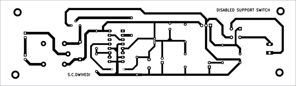
An actual-size, single-side PCB for the swap is proven in Fig. 3 and its part format in Fig. 4. After assembling the circuit on PCB, enclose it in an appropriate field. Join LDR in entrance of the field and prolong the foot swap to the disabled particular person’s chair utilizing a versatile wire.
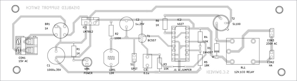
After correct set up, join 230V AC mains to main terminals of the transformer and 15V AC secondary terminals throughout CON1. The circuit is now prepared to make use of, supplied the LDR has been put in on the home switchboard and the foot swap has been prolonged as much as the disabled particular person’s chair.
Bonus. You’ll be able to watch the video of the tutorial of this DIY challenge
Obtain PCB and Element Structure PDFs: click on right here
S.C. Dwivedi is an electronics fanatic and circuit designer at EFY